In which we add the crystal, finish wiring and insert the chip.
This is part three of a short series describing in detail how to build an arduino clone from scratch for very little money. You can find the previous parts here:
Part 1
Part 2
Part 2.5 (circuit and parts list)
CRYSTAL OSCILLATOR CIRCUIT
The crystal circuit is used to allow the ATMega chip to accurately time intervals.
Components required:
- 1 × crystal – 16.0MHz U4 style low profile can
- 2 × 22pF ceramic capacitors
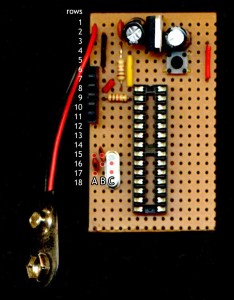
See the picture below for placement. As you can’t see where the crystal’s legs are placed, I’ve marked which holes they are in by two red dots. For clarity I’ve also marked where the capacitors’ legs attach also.
For extra clarity, from the picture:
Capacitor “A” connects to rows 15 and 17
Capacitor “B” connects to rows 15 and 16
Crystal “C” connects to rows 16 and 17.
Note that the crystal’s legs are set too wide to span two adjacent rows – I’ve just bent them in so they fit – it means the crystal’s case doesn’t sit flush to the board, but that doesn’t matter.
None of these components have a polarity so it doesn’t matter which way round they go.
FINAL CONNECTIONS
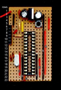
We’ve got all the componentry on the board now (apart from plugging in the ATMega chip!). Now it’s just a question of making a few more connections. See the following image and follow the list below:
Wire “A” connects row 7 to row 22 – now 7 and 22 are at +5V.
Wire “B” connects row 2 (GND) to 23. We now have power “rails” at the bottom of the board.
Wire “C” connects 22 back to row 14 (left side), i.e. attaches the ATMega’s VCC pin to +5V.
Wire “D” connects 23 back to row 15 (left side), i.e. attaches the ATMega’s GND pin to negative.
We also need to connect a couple of pins on the right side of the ATMega:
Wire “E” connects row 22 to 16 (right side), i.e. attaches the ATMega’s AVCC pin to +5V.
Wire “F” connects row 23 to 14 (right side), i.e. attaches the ATMega’s other GND pin to negative.
Capacitor “G” connects between the bottom power “rails”, i.e. row 22 & 23.
Now’s probably a good time to list the pins of the chip in more detail. I’ll list them by the row number of the board, starting with the left side:
Row Pin Description
8 RESET - we've wired this to the reset button
9 RXD (pin 0) - this connects to the serial connector on the left for uploading your "sketches".
10 TXD (pin 1) - again, connects to the serial connector.
11 pin 2
12 pin 3
13 pin 4
14 VCC - connected to +5V
15 GND - connected to negative
16 CLOCK1 - connected to the crystal
17 CLOCK2 - connected to the crystal
18 pin 5
19 pin 6
20 pin 7
21 pin 8
Now the right side of the chip:
Row Pin Description
8 Analogue pin 5
9 Analogue pin 4
10 Analogue pin 3
11 Analogue pin 2
12 Analogue pin 1
13 Analogue pin 0
14 GND - connected to negative
15 AREF - we're leaving this unconnected
16 AVCC - connected to +5V
17 pin 13
18 pin 12
19 pin 11
20 pin 10
21 pin 9
As you’ll probably see, all the pin names are the ones available on your “real” arduino. So, for example, if we wanted to test the board using the “blink” sketch, we could hook up an LED (plus current limiting resistor) to pin 13 on row 17, right hand side (“real” arduino boards already have an LED connected) and test it.
ADDING A HEADER FOR PIN-OUTS
Normally if we’re building a dedicated circuit we’ll want to solder our connections to particular input / output pins on the ATMega directly to the stripboard. However for convenience of testing and burning the bootloader, I’m adding a small female header to the board. This step is optional, especially if you are using an ATMega which has already had an arduino bootloader burned onto it.
We’re essentially just exposing three pins – 13,12 and 11. Connect it to rows 17,18 and 19, on the right hand edge of the stripboard.
Now plug the ATMega chip in, carefully, to its socket, making sure the little notch on the top edge matches the notch on the socket (i.e. at the top, nearest to the power supply circuit). Usually chips come with their feet splayed a little wider than the socket – just gently bend them in on a flat surface if this is the case. When you’re inserting the chip make sure none of the legs get folded under rather than going into their sockets – it’s an easy thing to do if you’re not careful.
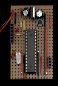
So, we’re finished as far as the hardware is concerned. Here’s the finished product:
–
And that wraps up this installment. We now have a board which is almost ready. So the next post will be an interesting one – how to burn the bootloader, which a lot of people seem to have problems with (especially using an Uno to do so), and after that we can then cover how to upload our programs to it.
Next post is now up here: http://www.martyndavis.com/?p=188


Right this going in my Cybot…. remember those? Goodbye proprietary, hello Open!
This is an excellent series, I am looking forward to the next installment!
for those interested you can buy a kit of parts minus the vero(strip)board from these people http://www.oomlout.co.uk/component-bundle-for-arduino-compatible-arcb-p-227.html for around uk £7.50